- IC型号
深圳市华兴微电子有限公司

- 营业执照:已审核经营模式:所在地区:广东 深圳企业网站:
http://www.hxw-rf.com/
收藏本公司 人气:502547
联系方式
- 地址:深圳市福田区华强广场A座14B
- 联系人:王小姐
- 电话:0755-83002107
- 传真:0755-83335110
- 手机:18476741579
- QQ:

- E-mail:2880509077@qq.com
供应HMC987LP5E
- 产品价格:
- ¥3/ 1pcs
¥3/ 10pcs
¥3/ 100pcs
¥3/ 1k
¥3/ 10k
- 厂 家:
- HITTITE
- 封 装:
- 绝对进口原装
- 批 号:
- 13+
- 数 量:
- 58000
产品咨询直线:0755-83002107
产品详细说明
| Clock Rate (GHz) | Function | Input | Output | Phase Jitter (12 K to 20 MHz) | Rise / Fall Time (ps) | Channel Skew (ps) | Power Supply (V) |
|---|---|---|---|---|---|---|---|
| DC - 8 | 1:9 Fanout Buffer | LVPECL, LVDS, CML, CMOS | LVPECL | 8 fsRMS | 65 | 3.1 | 3.3 |
![]()
To order this product direct from Digi-Key click here.
Features
• Ultra Low Noise Floor: -166 dBc/Hz |
Typical Applications
• SONET, Fibre Channel, |
Functional Diagram |
General DescriptionThe HMC987LP5E 1-to-9 fanout buffer is designed for low noise clock distribution. It is intended to generate relatively square wave outputs with rise/ fall times < 100 ps. The low skew and jitter outputs of the HMC987LP5E, combined with its fast rise/ fall times, leads to controllable low-noise switching of downstream circuits such as mixers, ADCs/DACs or SERDES devices. The noise floor is particularly important in these applications, when the clocknetwork bandwidth is wide enough to allow squarewave switching. Driven at 2 GHz, outputs of the HMC987LP5E have a noise floor of -166 dBc/Hz, corresponding to a jitter density of 0.6 asec/rtHz - or 50 fs over an 8 GHz bandwidth. The input stage can be driven single-ended or differentially, in a variety of signal formats (CML, LVDS, LVPECL or CMOS), AC or DC coupled. The input stage also features adjustable input impedance. It has 8 LVPECL outputs, and 1 CML output with adjustable swing/power-level in 3 dB steps. Individual output stages may be enabled or disabled for power-savings when not required using either hardware control pins, or under control of a serial-port interface. |
||

相关产品更多>>
-

- 供应HMC890LP5E
- ¥3
-
- 供应HMC891LP5E
- ¥3
-
- 供应HMC892LP5E
- ¥3
-
- 供应HMC893LP5E
- ¥3
-
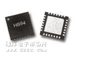
- 供应HMC894LP5E
- ¥3
-
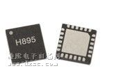
- 供应HMC895LP4E
- ¥3
-
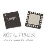
- 供应HMC896LP4E
- ¥3
-
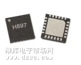
- 供应HMC897LP4E
- ¥3