- IC型号
深圳市德宏源电子有限公司

- 营业执照:已审核经营模式:贸易/代理/分销所在地区:广东 深圳企业网站:
http://www.vigsou.com
收藏本公司 人气:124315
联系方式
- 地址:深圳市福田区彩田路彩虹新都彩霞阁31F室
- 联系人:市场部/销售部/销售部
- 电话:0755-83218556/0755-83219929/0755-83211827
- 传真:0755-83219926
- 手机:13510200348//
- QQ:


- E-mail:llk204@163.com
产品分类
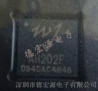
供应WJ射频和微波驱动放大器AH202F
产品详细说明
供应WJ射频和微波驱动放大器AH202F,全新原装公司现货!
Product Features 30 – 2200 MHz 17 dB Gain @ 900 MHz +30 dBm P1dB +47 dBm Output IP3 Single Positive Supply Internally Matched Lead-free/RoHS-compliant 6x6mm QFN SMT package
Applications Mobile Infrastructure CATV / DBS Optimal for VHF / UHF broadband applications Defense / Homeland Security
Product Description
The AH202 is a 1-Watt driver amplifier that offers excellent dynamic range in a low-cost, lead-free/RoHS-compliant 6x6 mm 28-pin QFN surface-mount package. This device provides its optimum P1dB and OIP3 performance when biased at + 11 V; It can also be biased as low as +9 V for lower power applications.
The backside metalization provides excellent thermal dissipation while allowing visible evidence of solder reflow across the bottom of the package on a SMT board. Superior thermal design allows the product an MTTF of over 100 years at a mounting temperature of +85º C. All devices are 100% RF & DC tested.
The product is targeted for use as a driver amplifier for wireless infrastructure or CATV applications where high linearity and medium power is required.
Functional Diagram
Function
Pin No.
Input
3
No Connect
7
Output/Bias
19
No Connect or Ground
All other pins
Ground
Backside Paddle
Specifications (1) Parameters Units Min Typ Max
Operational Bandwidth
MHz
30
2200
Test Frequency
MHz
800
Gain
dB
14
17
Input Return Loss
dB
20
Output Return Loss
dB
18
Output P1dB
dBm
+29
+30
Output IP3 (2)
dBm
+45
+47
Noise Figure
dB
2.5
IS-95 Channel Power (3)
@ -45dBc ACPR
dBm
+24
Operating Current Range
mA
330
390
Supply Voltage
V
+11
1. Test conditions unless otherwise noted: 25ºC, Vdd = 11 V in a 50-Ω unmatched fixture.
2. 3OIP measured with two tones at an output power of +10 dBm/tone separated by 10 MHz. The suppression on the largest IM3 product is used to calculate the 3OIP using a 2:1 rule.
3. IS-95, 9 Channels Forward, Pk/Avg Ratio = 11.5 dB at a .001% probability, ±885 kHz offset, 30 kHz bandwidth, Channel BW = 1.23 MHz.
Absolute Maximum Rating Parameter Rating
Storage Temperature
-55 to +125 C
DC Voltage
+13 V
RF Input Power (continuous)
+16 dBm
Thermal Resistance, Rth
18 C/W
Maximum Junction Temperature
+160 C
Operation of this device above any of these parameters may cause permanent damage.
Typical Performance (4) Parameters Units Typical
Frequency
MHz
900
1900
2140
Gain
dB
17
15
15
Input Return Loss
dB
20
17
8
Output Return Loss
dB
18
10
13
Output P1dB
dBm
+30
+29.7
+29.4
Output IP3
dBm
+47
+46
+45.5
Noise Figure
dB
2.8
3.8
4.8
IS-95 Channel Power (3)
@ -45dBc ACPR
dBm
+24
+23
-
WCDMA Channel Power (5)
@ -45dBc ACLR
dBm
-
-
+20.5
Supply Bias
+11 V @ 330 mA
4. Data reflects performance of a typical AH202 in an application circuit including associated circuit board and passive component losses.
5. 3GPP W-CDMA, Test Model 1, +32 DPCH, Pk/Avg Ratio = 8.5 dB at a 0.01% probability, ±5 MHz offset, Integrated Channel BW = 3.84 MHz.
