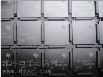
- IC型号
北京凌峰伟业科技有限公司

- 营业执照:已审核经营模式:经销商所在地区:北京 北京市企业网站:
http://www.lfwykj.com/
收藏本公司 人气:159616
联系方式
- 地址:北京市海淀区知春路罗庄西里13号东达写字楼227室
- 联系人:王小姐
- 电话:010-82059633
- 传真:010-82059633
- 手机:18618126725
- QQ:

- E-mail:lfwyic@126.com
产品分类
推荐产品
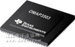
供应OMAP3503DCUS,处理器OMAP3503DCUS,北京现货OMAP3503DCUS
产品详细说明
供应OMAP3503DCUS,处理器OMAP3503DCUS,北京现货OMAP3503DCUS
BitmapPictPictPictPictPictPictPict
|
Texas Instruments | |
| 产品种类: | 处理器 - 专门应用 | |
| RoHS: | 详细信息 | |
| 工作电源电压: | 1.8 V, 3 V | |
| 最大工作温度: | + 70 C | |
| 安装风格: | SMD/SMT | |
| 封装 / 箱体: | BGA-423 | |
| 封装: | Tray | |
| 核心: | ARM CortexA8 | |
| 数据总线宽度: | 32 bit | |
| 数据 RAM 大小: | 64 KB | |
| 数据 ROM 大小: | 112 KB | |
| 接口类型: | 1-Wire, I2C, MMC, McBSP, McSPI, SDIO, UART, USB | |
| 最大时钟频率: | 600 MHz | |
| 最小工作温度: | 0 C | |
| 可编程输入/输出端数量: | 170 | |
| 定时器数量: | 12 32-bit GP, 2 32-bit WD | |
| 处理器系列: | OMAP35x | |
| 程序存储器大小: | 32 KB, 256 KB | |
| 程序存储器类型: | Flash | |
| 工厂包装数量: | 90 |
OMAP3503DCUS说明
OMAP3515 and OMAP3503 high-performance, applications processors are based on the enhanced OMAP™ 3 architecture.
The OMAP™ 3 architecture is designed to provide best-in-class video, image, and graphics processing sufficient to support the following:
・ Streaming video
・ 3D mobile gaming
・ Video conferencing
・ High-resolution still image
The device supports high-level operating systems (OSs), such as:
・ Linux
・ Windows CE
This OMAP device includes state-of-the-art power-management techniques required for high-performance mobile products.
The following subsystems are part of the device:
・ Microprocessor unit (MPU) subsystem based on the ARM Cortex™-A8 microprocessor
・ POWER SGX ™ subsystem for 3D graphics acceleration to support display and gaming effects (3515 only)
・ Camera image signal processor (ISP) that supports multiple formats and interfacing options connected to a wide variety of image sensors
・ Display subsystem with a wide variety of features for multiple concurrent image manipulation, and a programmable interface supporting a wide variety of displays. The display subsystem also supports NTSC/PAL video out.
・ Level 3 (L3) and level 4 (L4) interconnects that provide high-bandwidth data transfers for multiple initiators to the internal and external memory controllers and to on-chip peripherals
The device also offers:
・ A comprehensive power and clock-management scheme that enables high-performance, low-power operation, and ultralow-power standby features. The device also supports SmartReflex™ adaptative voltage control. This power management technique for automatic control of the operating voltage of a module reduces the active power consumption.
・ Memory stacking feature using the package-on-package (POP) implementation (CBB package only)
OMAP3515/03 devices are available in a 515-pin PBGA package (CBB suffix) and a 423-pin PBGA package (CUS suffix). Some features of the CBB package are not available in the CUS package.
特性
・ OMAP3515/03 Applications Processor:
o OMAP™ 3 Architecture
o MPU Subsystem
§ Up to 720-MHz ARM Cortex™-A8 Core
§ NEON™ SIMD Coprocessor
o POWERVR SGX™ Graphics Accelerator (OMAP3515 Device Only)
§ Tile Based Architecture delivering 10 MPoly/sec
§ Universal Scalable Shader Engine: Multi-threaded Engine Incorporating Pixel and Vertex Shader Functionality
§ Industry Standard API Support: OpenGLES 1.1 and 2.0, OpenVG1.0
§ Fine Grained Task Switching, Load Balancing, and Power Management
§ Programmable High Quality Image Anti-Aliasing
o Fully Software-Compatible With ARM9™
o Commercial and Exteneded Temperature Grades
・ ARM Cortex™-A8 Core
o ARMv7 Architecture
§ Trust Zone®
§ Thumb®-2
§ MMU Enhancements
o In-Order, Dual-Issue, Superscalar Microprocessor Core
o NEON™ Multimedia Architecture
o Over 2x Performance of ARMv6 SIMD
o Supports Both Integer and Floating Point SIMD
o Jazelle® RCT Execution Environment Architecture
o Dynamic Branch Prediction with Branch Target Address Cache, Global History Buffer, and 8-Entry Return Stack
o Embedded Trace Macrocell (ETM) Support for Non-Invasive Debug
・ ARM Cortex™-A8 Memory Architecture:
・ 16K-Byte Instruction Cache (4-Way Set-Associative)
・ 16K-Byte Data Cache (4-Way Set-Associative)
・ 256K-Byte L2 Cache
・ 112K-Byte ROM
・ 64K-Byte Shared SRAM
・ Endianess:
・ ARM Instructions - Little Endian
・ ARM Data ― Configurable
・ External Memory Interfaces:
・ SDRAM Controller (SDRC)
o 16, 32-bit Memory Controller With 1G-Byte Total Address Space
o Interfaces to Low-Power Double Data Rate (LPDDR) SDRAM
o SDRAM Memory Scheduler (SMS) and Rotation Engine
・ General Purpose Memory Controller (GPMC)
o 16-bit Wide Multiplexed Address/Data Bus
o Up to 8 Chip Select Pins With 128M-Byte Address Space per Chip Select Pin
o Glueless Interface to NOR Flash, NAND Flash (With ECC Hamming Code Calculation), SRAM and Pseudo-SRAM
o Flexible Asynchronous Protocol Control for Interface to Custom Logic (FPGA, CPLD, ASICs, etc.)
o Nonmultiplexed Address/Data Mode (Limited 2K-Byte Address Space)
・ System Direct Memory Access (sDMA) Controller (32 Logical Channels With Configurable Priority)
・ Camera Image Signal Processing (ISP)
・ CCD and CMOS Imager Interface
・ Memory Data Input
・ RAW Data Interface
・ BT.601/BT.656 Digital YCbCr 4:2:2 (8-/16-Bit) Interface
・ A-Law Compression and Decompression
・ Preview Engine for Real-Time Image Processing
・ Glueless Interface to Common Video Decoders
・ Histogram Module/Auto-Exposure, Auto-White Balance, and Auto-Focus Engine
・ Resize Engine
o Resize Images From 1/4x to 4x
o Separate horizontal/Vertical Control
・ Display Subsystem
・ Parallel Digital Output
o Up to 24-Bit RGB
o HD Maximum Resolution
o Supports Up to 2 LCD Panels
o Support for Remote Frame Buffer Interface (RFBI) LCD Panels
・ 2 10-Bit Digital-to-Analog Converters (DACs) Supporting:
o Composite NTSC/PAL Video
o Luma/Chroma Separate Video (S-Video)
・ Rotation 90-, 180-, and 270-degrees
・ Resize Images From 1/4x to 8x
・ Color Space Converter
・ 8-bit Alpha Blending
・ Serial Communication
・ 5 Multichannel Buffered Serial Ports (McBSPs)
o 512 Byte Transmit/Receive Buffer (McBSP1/3/4/5)
o 5K-Byte Transmit/Receive Buffer (McBSP2)
o SIDETONE Core Support (McBSP2 and 3 Only) For Filter, Gain, and Mix Operations
o Direct Interface to I2S and PCM Device and TDM Buses
o 128 Channel Transmit/Receive Mode
・ Four Master/Slave Multichannel Serial Port Interface (McSPI) Ports
・ High-Speed/Full-Speed/Low-Speed USB OTG Subsystem (12-/8-Pin ULPI Interface)
・ High-Speed/Full-Speed/Low-Speed Multiport USB Host Controller
o 12-/8-Pin ULPI Interface or 6-/4-/3-Pin Serial Interface
o Supports Transceiverless Link Logic (TLL)
・ One HDQ/1-Wire Interface
・ Three UARTs (One with Infrared Data Association [IrDA] and Consumer Infrared [CIR] Modes)
・ Three Master/Slave High-Speed Inter-Integrated Circuit (I2C) Controllers
・ Removable Media Interfaces:
・ Three Multimedia Card (MMC)/ Secure Digital (SD) With Secure Data I/O (SDIO)
・ Comprehensive Power, Reset, and Clock Management
・ SmartReflex™ Technology
・ Dynamic Voltage and Frequency Scaling (DVFS)
・ Test Interfaces
・ IEEE-1149.1 (JTAG) Boundary-Scan Compatible
・ Embedded Trace Macro Interface (ETM)
・ Serial Data Transport Interface (SDTI)
・ 11 32-bit General Purpose Timers
・ 2 32-bit Watchdog Timers
・ 1 32-bit 32-kHz Sync Timer
・ Up to 188 General-Purpose I/O (GPIO) Pins (Multiplexed With Other Device Functions)
・ 65-nm CMOS Technology
・ Package-On-Package (POP) Implementation for Memory Stacking (Not Available in CUS Package)
・ Descreet Memory Interface (Not Available in CBC Package)
・ Packages:
・ 515-pin s-PBGA Package (CBB Suffix), .5mm Ball Pitch (Top), .4mm Ball Pitch (Bottom)
・ 515-pin s-PBGA Package (CBC Suffix), .65mm Ball Pitch (Top), .5mm Ball Pitch (Bottom)
・ 423-pin s-PBGA Package (CUS Suffix), .65mm Ball Pitch
・ 1.8-V I/O and 3.0-V (MMC1 only), 0.975-V to 1.35-V Adaptive Processor Core Voltage, 0.975-V to 1.35-V Adaptive Core Logic Voltage
・ Applications:
・ Portable Navigation Devices
・ Portable Media Player
・ Advanced Portable consumer Electronics
・ Digital TV
・ Digital Video Camera
・ Portable Data Collection
・ Point-of-Sale Devices
・ Gaming
・ Web Tablet
・ Smart White Goods
・ Smart Home Controllers
・ Ultra Mobile Devices